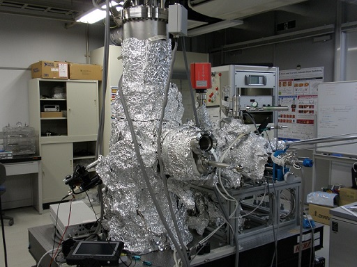
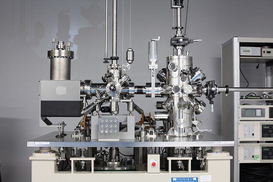
INTRODUCTION OF LABORATORY
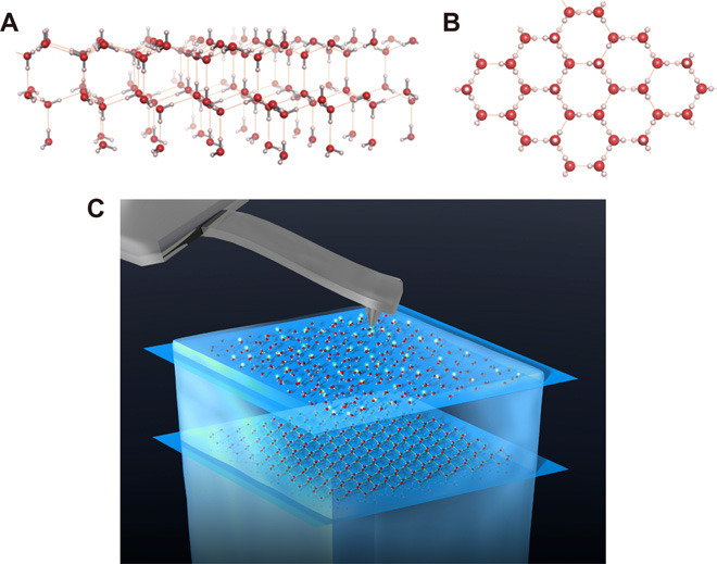
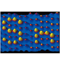
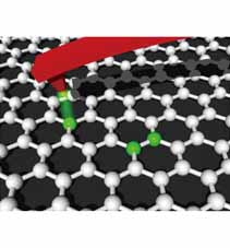
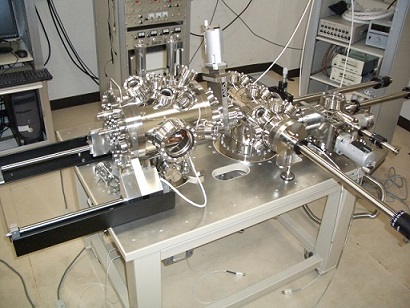
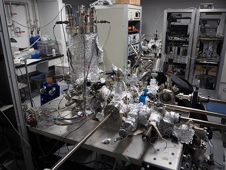
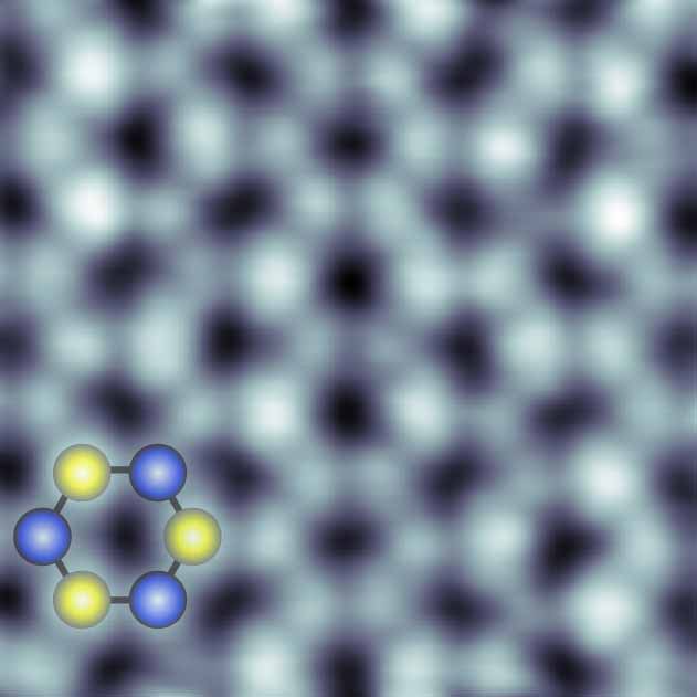
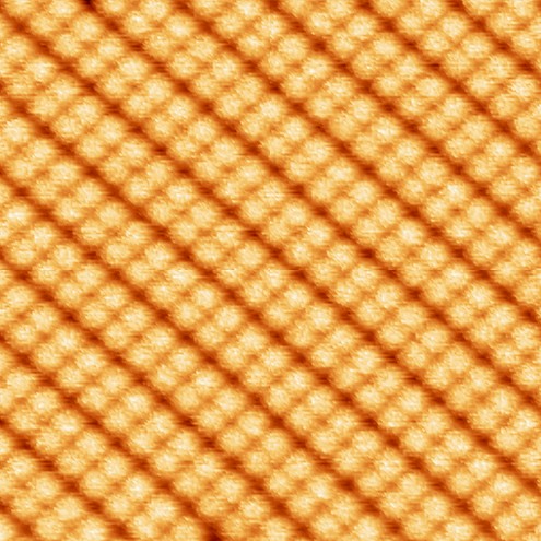
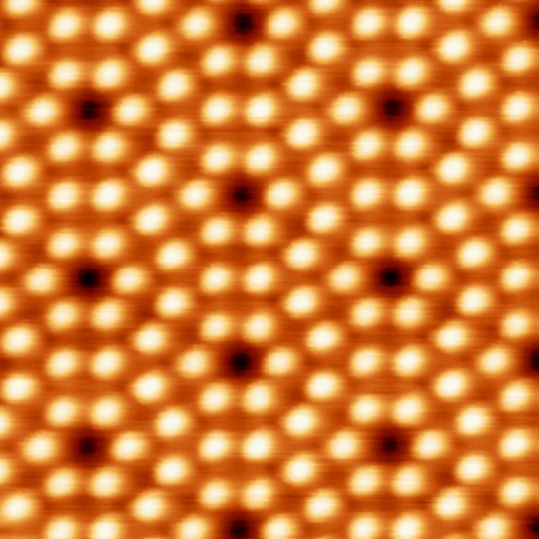
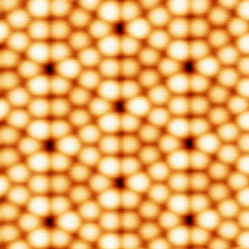
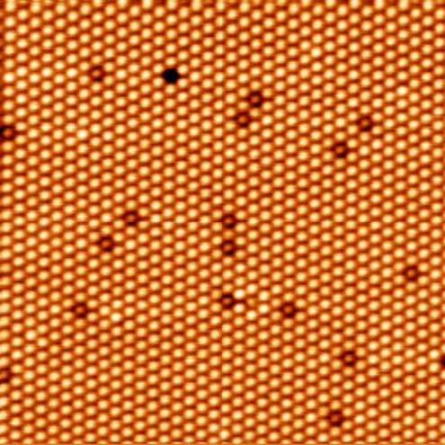
The ability to assemble nanostructures with unique and specific properties is a key technology for developing the next generation devices. For this goal, major success is anticipated through the bottom-up approach: an attempt to create such nano-devices from the atomic or molecular level instead of miniaturizing from the macroscopic world. In the bottom-up approach, the ultimate limit is to fabricate artificial nanostructures on surfaces by manipulating single atoms or molecules one by one. In our laboratory, we are developing such atom manipulation techniques as well as chemical identification and local characterization techniques using scanning probe microscopy (SPM). Our SPMs are based on Atomic force microscopy (AFM) that has wide applications, such as, insulator imaging and force measurements. Combination with Scanning tunneling microscopy (STM) allows us to access various physical/chemical quantities on identical atoms at the same time. We are also developing the new system to achieve higher spatial resolution and higher functionality.